The terms "gain equalization" and "gain flattening" come from the fiberoptic telecommunications field, where erbium-doped fibers are used to amplify the light traveling through the fiber. These amplifiers have a wavelength-dependent gain; i.e., some wavelengths are amplified more than others. A gain-flattening filter restores all wavelengths to approximately the same intensity. Erbium-doped fiber amplifiers (EDFA) operate in the 1530-1565 nm wavelength range.
7 b$ _0 l. x. A' SThis type of filter has many applications. For example, for visible wavelengths 380-780 nm, a filter could be constructed to convert any continuous-spectrum illuminant into white light; e.g., light from an ordinary light bulb could be filtered to produce almost pure white light.
* f) i# w$ H: j) iAn introduction of the design of this filter can be found in the paper
) W. C& ~. J* l3 `. BM. Tilsch, C.A. Hulse, K.D. Hendrix, R.B. Sargent, "Design and demonstration of a thin-film based gain equalization filter for C-band EDFAs", presented at the 1999 NFOEC conference./ j+ f+ Z/ m! l- `4 B# \7 ^1 w: u
The plot below shows the relative intensity of the EDFA output. If this were plotted on the logarithmic dB scale, the output would have a range of 8 dB.
G. k) I( [4 }' ]6 v+ K P8 W+ E% U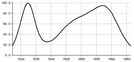
0 |0 p# I1 I7 z. C* S5 j$ k' l We will use TFCalc's optimization capabilities to design a gain-flattening reflection filter which will flatten (or equalize) the output of the EDFA so that it is flat with a tolerance of ±0.5 dB. In general, the tolerance is tighter for real filters. F7 C6 N4 w% [/ t
TFCalc has the capability of optimizing the product of the illuminant (EDFA) and the reflectance (or transmittance) of a coating. We want this product, which is the actual output of the filter, to be a flat as possible. As can be seen from the plot shown above, even if the filter reflects (or transmits) a 100% at the endpoints (1527.3 and 1566.3 nm), the output would only be about 20%. Hence, for the entire wavelength range, the flattened output of the filtered EDFA can be no more than 20%. The design becomes somewhat easier if the target output is less than 20%.
: m2 m% }+ s0 p6 k. S0 |, j: t$ oReflection Filter. G, n- f3 b2 S& P0 k' d
Tilsch et al studied the reflection filter in their paper. To design such a filter, we started with the initial 100-layer design (HL)^50, where H represents 1.2 QWOT of index 2.25 and L represents 1.2 QWOT of index 1.45. The reference wavelength is 1530 nm. The substrate has index 1.44. We design this for normal incidence; in reality, the filter will be positioned at a small angle. For the optimization target we use 0 L5 k( C" `7 c" y
EDFA * Reflectance = 17.5% for wavelengths from 1527.3 to 1566.3) t( v7 O/ D b7 c: r# C* _" F
A total of 201 equally-spaced targets are used. To make the output as flat as possible, we use power=16 during optimization. The result is a 91-layer design. In white light, the performance of the filter is shown below.
$ W3 k1 n) ]$ \9 q5 X% o8 M6 X0 d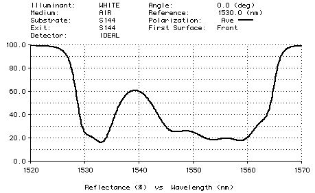
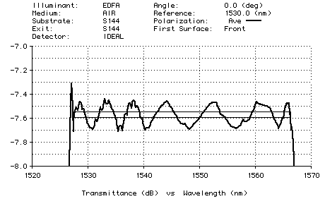
! w( Y. _; M" y7 F$ x6 B The plot below shows the output of the filtered EDFA. If this is plotted on a dB scale, it becomes apparent that the design, if it could be produced without errors, meets the ±0.5 dB requirement.
6 d5 @: `) B3 ?: ~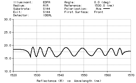 % ^: A0 P! ^* q/ U: u % ^: A0 P! ^* q/ U: u
8 N p# [4 L7 s$ e
Transmission Filter
8 Z3 V7 V2 X. n1 E1 UTo discover whether there is any advantage in using a transmission filter, we decided to design one. Most of the details are the same as for the reflection filter. However, this time we started with the 101-layer design (HL)^50 H. The target is % D, v( i9 |; z2 T2 V
EDFA * Transmittance = 17.5% for wavelengths from 1527.3 to 1566.3. m: v9 J2 n0 B0 _( [/ f
We used one continuous target. Again, we use power=16. By constraining the layer thicknesses to be greater than 0.5 QWOT during optimization, we discover a 101-layer design having a very flat (less than ±0.12 dB) output, as displayed below on a dB scale. % o# v* ?8 a9 g, Z! H$ {3 |8 i M* J
; I. p" p3 k3 k& Y% Q, `
0 a2 T; ?/ q# EManufacturability
1 n9 r& `# a% [# p9 X) w) n1 RBy randomly varying the thickness of layers, TFCalc can determine the manufacturability of a design. For the designs mentioned in the Tilsch et al paper, a maximum error of 0.05% is required for production. Note that, using this error limit, if a layer is 100 nm thick, then the thickness must be monitored to within ±0.5 angstrom! The plot below shows the range of the performance of the reflection filter for 1000 random designs when layers are allowed to vary uniformly by ±0.05%. 3 d- P L' s u2 n- K* |% L) |
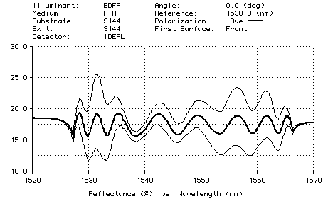 5 {* K! N$ o* ?6 b2 s' \* b0 S 5 {* K! N$ o* ?6 b2 s' \* b0 S
Even 0.05% seems barely acceptable. Using TFCalc's sensitivity optimization capability, we can try to find a design that is less sensitive to manufacturing errors. The procedure is rather slow, but the results may be worth the wait. We chose to optimize the sensitivity of 1000 random designs. On a 1 GHz Pentium, this requires several hours. Below is the sensitivity analysis of the improved design. Note that the optimizer has found a design that is significantly less sensitive to thickness errors. ; I4 a9 n; g+ k9 Z8 l8 o" ~
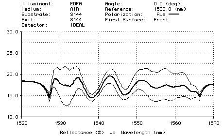
2 V. b9 V, O- O% b% e& H+ x Although the sensitivity optimization seems to work by making the performance of the filter flatter when the intensity of the EDFA is high, the optimizer actually does more. Numerical experiments show that, in general, merely designing a filter that is flatter where the EDFA intensity is high will still be very sensitive to thickness variations. The sensitivity optimization actual finds a less sensitive design, which also happens to have a flatter output at wavelengths where the EDFA has higher intensity.
# _4 u; T) Y6 q+ B4 UThis work is not nearly as exhaustive as in the Tilsch et al paper. However, it does show how optimizing the sensitivity can improve the performance of a design.
% V! s9 c5 R3 j6 u+ hHere are the two designs; Design 1 is the original reflection design; Design 2 is the reflection design optimized for sensitivity. The first layer is closest to the substrate and thickness is given in nm:
1 n6 _8 Z0 z v* B: [ }Material Design1 Design2
; q v1 b) F( J! m7 o( qN225 173.22 183.23
- @- N, Z& H f! G+ m; |N145 266.11 283.45
. D+ E8 r) F3 ^N225 170.37 187.68- d2 Y$ o+ ]# C% E1 {
N145 281.70 310.91
, I: B1 |! p* ]) P& J1 i% A2 NN225 241.67 232.70
2 U' M% M l9 ?7 q# CN145 499.80 486.55
, v/ X9 b( W3 `* [5 eN225 149.42 123.93
; J+ a$ n2 Y) q gN145 216.86 239.551 I: ? Y5 \& P! M% ^
N225 170.23 182.06
# R, Y0 ]6 O4 h% @* ^/ [N145 276.29 300.51
+ x+ l0 s/ t9 G8 h" GN225 162.25 185.722 ?2 L, O! ^7 s* w% k
N145 260.42 264.95
8 ?$ U( I$ m6 O; {! B' P+ ?# u+ Y1 ~, ZN225 176.10 151.72
$ e8 T4 y. N3 N$ R) V2 qN145 249.71 215.61
$ Z: b% `2 k5 k( j. YN225 389.76 404.62% z* z8 E! G' T% f
N145 244.24 250.29
7 E" K7 K/ m; X! W! f# BN225 176.51 176.04- {. A. V' l! q
N145 269.84 258.26
' |, W* s8 A: _2 ^N225 172.68 161.16
2 v# l% U f# W& A/ qN145 351.00 358.607 S% u9 T7 S1 A6 G+ H
N225 318.17 316.63, h4 @) Z2 X3 Q, `/ Y
N145 285.93 279.08
; g- p/ }3 F5 x/ Q) ]% F, HN225 158.51 181.70: ?6 T8 ], ~1 d% k+ n$ p+ c5 Q
N145 246.70 282.898 O) O7 n1 W) J7 s8 P
N225 177.51 169.19
8 i* V) `; _4 d' [N145 290.04 253.96) t; t: H' j. I" {- |; v
N225 166.26 165.89
/ j: G( G0 Q+ k4 H1 v/ P: R2 [N145 265.69 263.71
/ @6 s' V4 ^( W# |+ F9 AN225 187.39 176.44
4 s6 L7 E; P* X: |% _2 K. d+ m; {N145 311.12 322.47( P: @. e3 y3 F* s8 R: [: d
N225 266.31 283.071 b5 I, C+ a) @; K2 ]7 H
N145 353.44 322.817 T* x, r5 |9 _! J8 N5 ~7 ^
N225 183.75 179.50' c* o4 _6 V! E
N145 268.79 273.764 o4 n$ v2 }1 }/ m4 {) r& i
N225 177.71 179.477 A, L Z" {# B( N) B, H4 H7 u. w
N145 267.34 275.20$ b$ B: t! C1 t
N225 180.82 186.318 U+ o: N" ~' [, n8 Z+ c b
N145 265.61 285.18
1 H8 J% ?: T9 I; G+ l) }$ r$ u& ?N225 179.56 191.58
/ h. d r' j, C: H3 }/ a) zN145 310.69 307.51
8 i% m; Y' A1 C3 tN225 201.44 191.857 C$ x( S) t8 }
N145 337.80 335.97
: I( e7 O% N+ g- eN225 546.46 539.712 k3 _9 \7 F1 z! Q
N145 419.51 418.70( n4 A: a- j6 |5 B1 @: }% ?, o
N225 180.85 182.18
, e/ V9 C) B! F+ c! ]2 p" NN145 261.04 270.87/ Q( q G. n/ M# L
N225 173.18 179.08
/ E1 E. X, x) @5 W# n, D% y3 p# iN145 264.37 276.37) R$ D6 Z9 U) D; l0 @
N225 172.93 185.79
) t, |1 k2 A$ A$ p' AN145 264.15 256.11
( C2 x% L8 G3 o' x9 n( IN225 175.67 168.30
5 w# P% c9 y+ c: Y3 u! D. `: ~N145 265.07 260.124 P( \0 G/ x1 _# ?6 D& F' T
N225 178.47 199.99 B" V) J( |4 E2 h6 v' C
N145 251.01 244.43' J9 }+ I% i( z3 X& g- o) s8 ^0 a
N225 182.79 199.316 w& c& @9 E0 J! T+ c1 H
N145 596.29 582.84
5 o+ ~0 f8 B# `N225 115.52 114.77, s8 x+ ^' K+ i/ V$ g" E" f+ p
N145 244.92 217.389 a) H( A" \; O$ X/ \
N225 173.55 177.190 P9 g: n- @2 J$ s6 w
N145 263.13 271.27) S$ P3 }& |2 n) G
N225 168.53 174.835 p* O* s* B/ f) ^3 u# N
N145 265.62 276.17* G4 t4 [: v8 I
N225 172.31 179.17
1 ]% ]- \) T3 oN145 264.86 274.151 x" ^4 n$ A% k3 }! Z# J/ w
N225 175.52 180.52
" v! Z) X, ?, D9 R/ r2 m* n% IN145 280.45 288.85
( |* ]! z. s0 `+ F( KN225 176.08 183.838 A# m A4 h6 d, T) |* R( X0 A
N145 243.23 239.70
2 G6 z+ O. r: NN225 245.25 215.08
4 _3 C+ x" h$ H( G6 |- t2 R5 tN145 177.49 231.26) @1 E( Y& D7 Z& \( F n+ h
N225 358.93 358.44/ y( x) Z; G! j& j2 n
N145 262.76 255.62
: S7 O3 v6 M7 u) oN225 176.24 171.92
8 U! W" Q/ A+ a7 y( C( q: uN145 245.65 223.474 f/ K1 e+ l4 S& Y% h& n: W+ s0 o
N225 166.69 160.65; R* Q. t" y3 `9 Z
N145 255.30 259.856 s: n( ~, U6 Z& W; I# V
N225 165.34 169.67' g5 j1 P' S3 g8 k: `3 Z
N145 256.16 275.05
5 T. ^/ u1 L2 P/ d4 q2 a3 q6 {% V& }N225 412.72 403.735 y4 F4 G& Z* `6 i! b8 C3 Y
N145 239.67 218.934 Q8 \, @" _ I
N225 175.49 175.58* d( L1 j7 n0 [0 W. i
N145 273.85 297.29
6 j6 g7 i+ G1 X. \N225 140.82 169.58, a0 w6 X5 Z. p1 h% G
N145 297.28 309.52+ W8 d" {" y2 v1 u8 ?. V
N225 219.98 193.75( Y5 I" X; K% N& ?
N145 493.44 484.74
% k8 ?) `7 B1 D9 a" s5 f* l1 XN225 168.57 157.29
* f8 K* o* S+ @5 Z( ^% @: |N145 282.43 319.13$ k7 B: f( H( v
N225 175.48 186.11
4 b- V% D- f% I8 v+ U8 X/ L+ vN145 274.12 303.92( g6 l9 N8 F' `# O# e! V o$ @
N225 173.02 181.17 |
 发表于 2007-5-14 21:26:05
 提升卡
提升卡 置顶卡
置顶卡 沉默卡
沉默卡 喧嚣卡
喧嚣卡 变色卡
变色卡 抢沙发
抢沙发 显身卡
显身卡