[size=+3]Broadband Antireflection Graded-Index Coating / k" m+ }, Z) R
[ Contents ] [ Index ] [ Home ] , y2 g9 }, ? K' \% s) C
In an important 1962 paper,
: _, B4 Q! ^) L2 W+ QPeter H. Berning, "Use of Equivalent films in the design of infrared multilayer antireflection coatings", Journal of the Optical Society of America, Vol. 52(4), pp. 431-436 (April 1962).
5 C- i4 F9 |) none of the coatings discussed by the author is a step-graded-index antireflection coating for germanium. This coating consists of 20 quarter-wave layers whose indices vary linearly from 1.35 (the lowest practical index available) to 4 (the index of germanium), as illustrated below.
9 V" V2 K7 X% C8 D `; y% t7 _! \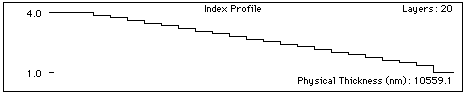
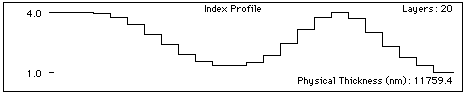
; d2 v! k4 N$ v! d5 k4 b$ w% b The coating has a very broad wavelength range over which the reflectance is low. The question arises: is the linear profile the best possible? We can use optimization to explore this problem. Here we use a feature unique to TFCalc -- the capability of optimizing the reflective index while keeping the optical thickness fixed. We use one continuous optimization target: R=0 for 3-20 microns. To make the reflectance as flat as possible, we set the power in the merit function to 16. Surprisingly, the resulting index profile looks like part of a sine curve: 8 ]& _( P9 f5 @1 T5 F7 t
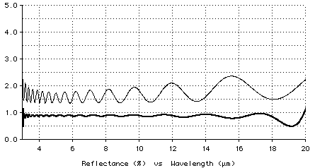
2 r d( [: W9 p3 v0 P5 i: j: z The performance of the optimized design is significantly better. The reflectances of the two designs are shown below. , ~- C. W" ^! o$ @1 w" g' m* k1 @
 8 {& E9 n2 [( h- V- T* P! R5 c! w 8 {& E9 n2 [( h- V- T* P! R5 c! w
# }9 _) x i+ h# c7 E; @Here is the list of refractive indices in the optimized design, starting with the layer closest to the germanium substrate:
' [8 L2 m' M6 P6 O2 c$ m! q6 N# J 1 3.9356' ~" F* b) m E& S
2 3.74822 N# Z. ~. t7 u! b9 i, `
3 3.3986- G5 u) ^, W2 a1 i/ x! M
4 2.9121& T, Q0 t9 l( `; M
5 2.3790# n0 W* \' D- N+ z2 t- ~2 m
6 1.9044
) D/ {: \. i. g# D1 K0 ?2 q( | 7 1.55981 b5 M4 o: h! l9 Y( |* ^
8 1.3726
P' b7 F0 X# v+ X& I( Y- r$ Z 9 1.35009 W6 l& M9 W1 f, y5 F: d# L+ P$ r
10 1.5042
7 e) }3 v7 k3 q, W3 Y 11 1.8606
% H4 n+ N. I$ ]& ~5 s0 k" R7 c 12 2.4315
+ p2 ?4 B" m% S8 G# M 13 3.1456
- z. A8 z- D% `0 `# N 14 3.7738
" y+ V7 _3 w: b3 Z, M+ f 15 4.0000
- @7 x F6 q" v$ v 16 3.6871
) x- d/ d/ R9 @, L 17 3.0181
3 A$ Y7 l6 K2 F" ?, u2 [. [ 18 2.3016
& L! I0 _1 k2 ~1 g9 @0 T w x& p) W 19 1.7310
7 w) @. J8 J6 _* o! \* o# y7 k 20 1.3500( t/ [, D( o. r9 a0 m1 X
The reference wavelength for the quarter-wave optical thickness is 5.217 microns, which is the midpoint, in the frequency scale, between 3 and 20 microns.
2 w1 `7 a, k8 CNote: by using more layers, designs with more cycles of the sine curve can be found. However, the additional cycles do not improve the performance as dramatically as above.
4 O$ {7 b" }& yDownload DesignYou may download the Berning design and watch how TFCalc optimizes it. You will need a real copy (i.e., not a demo) of TFCalc. Click here for the Windows or Macintosh file. This design assumes that you have a substrate called G whose index is 4. The G substrate was installed with the TFCalc software.
# \1 Y% q! N2 z* V* Z' ]0 g5 RWindows users, when they download this file, will have to save it to disk. Be sure to save it with extension ".TFD". |
 发表于 2007-5-14 21:17:24
 提升卡
提升卡 置顶卡
置顶卡 沉默卡
沉默卡 喧嚣卡
喧嚣卡 变色卡
变色卡 抢沙发
抢沙发 显身卡
显身卡